Jeep Circuits Build Guide
Five small boards that give the Pi engine RPM, a "key is on" signal, the starting-battery voltage, a UPS feed from the house bank, the amp remote turn-on, and the isolator solenoid driver. Every part comes from the parts inventory except one fuse holder and one spade terminal.
Build order
Go from easiest to hardest. Each build is tested on its own before the next one.
| Still to buy | For | Needed? |
|---|---|---|
| Inline blade fuse holder + 7.5 A fuse (16 AWG leads), ring terminal for the battery post | Board C | Required The only fuse left in the design. Nothing on hand can replace it. |
| ¼" insulated female spade | Tach wire onto the HEI cap's TACH terminal | Required for the tach |
| P6KE18A TVS (unidirectional) | Surge clamp at the X1209 input | Optional Add it later. Run without it for now (see the Gemini check). |
| 2-core shielded cable, ~3 m | Distributor to Board A | Optional Two wires twisted together (about 1 twist per inch) work fine here. |
The 1 A fuses for the ACC and starting-battery wires are no longer needed: their current-limiting resistor now sits at the far end of the wire instead (explained in Far-end resistors).
How to read the layouts
- The green drawings are the board seen from the parts side. Each gold ring is a hole. Columns are numbered across the top (0, 1, 2…) and rows down the side, so
(15,2)means column 15, row 2. - The thick coloured lines are the copper on the back: join those holes underneath with a bare wire or a solder bridge. One colour is one connection. Different colours must never touch.
- The clipped-off resistor and diode legs are perfect for the back-side wires. Lay one along the holes, solder it at every hole it crosses.
- Each part's legs go in exactly the holes shown. Bend them flat on the back toward their trace before soldering.
- The blue boxes are the screw terminals. They sit on the board edge with their screws facing outward.
- Diodes have a band. In the drawing the white band is at the cathode end. Match it. The P6KE12CA TVS diodes are bidirectional, so they go in either way.
- PC817 dot = pin 1. Pin 1 is top-left, pin 2 under it, pin 3 bottom-right, pin 4 top-right. The drawing marks the pin numbers in yellow.
board_layout.py holds these layouts as data and checks that every connection matches the schematic, that no two connections share a hole, and that nothing on the vehicle side crosses to the Pi side. From Board D v2 on, it also checks that no two different connections sit in side-by-side holes, except the legs of one part. Deliberate mistakes (a reversed diode, swapped PC817 pins, a bridged trace) were all caught.Board A: tach input + ACC sense
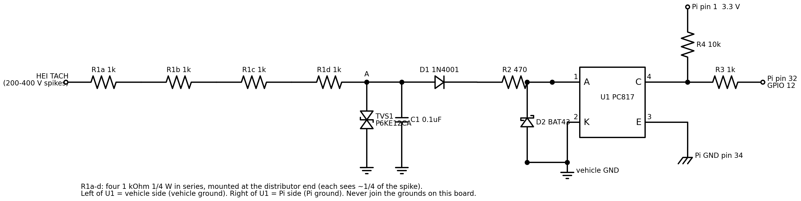
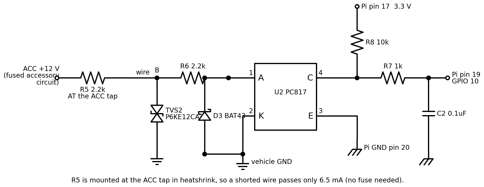
What it does. Each half has a PC817 optocoupler: a tiny LED and light sensor in one chip. The Jeep side lights the LED, and the Pi side only sees the light. Spikes from the ignition can't travel through light, so they can't reach the Pi. The yellow dashed line on the board is that barrier. Nothing crosses it except the chips.
- Tach (top half): every spark makes one pulse. A V8 sparks 4 times per turn of the crank, so RPM = pulses per second × 15. Idle is about 45 pulses a second.
- ACC (bottom half): key in Accessory or On lights the LED, and GPIO 10 reads LOW.
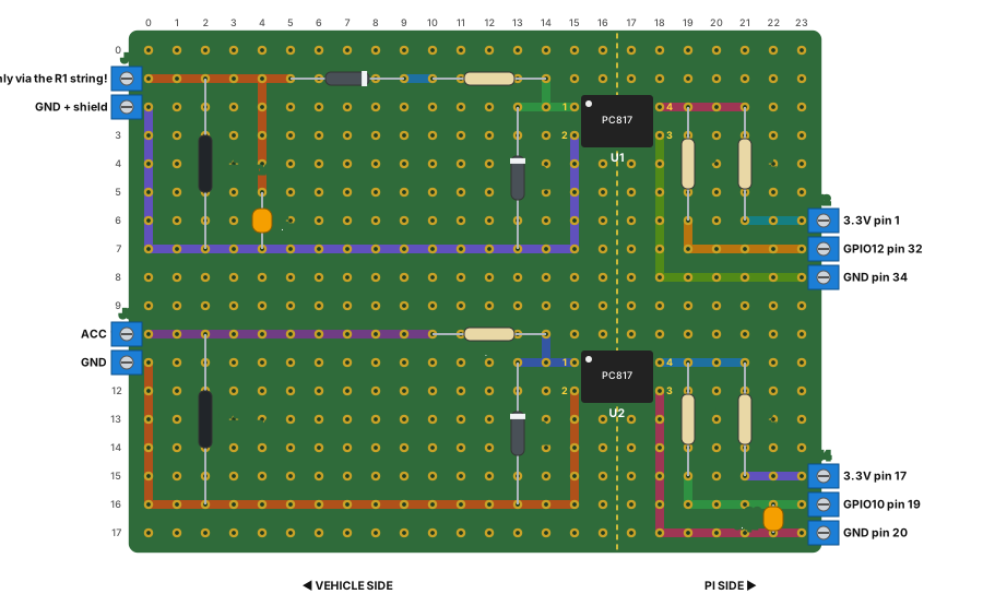
ELEGOO 5 × 7 cm board (24 × 18 holes). Left = vehicle side, right = Pi side.
Parts for Board A
| Ref | Part | Holes | Notes |
|---|---|---|---|
| U1, U2 | PC817 | pin 1 at (15,2) / (15,11) | Dot top-left |
| TVS1, TVS2 | P6KE12CA | (2,1)–(2,7) / (2,10)–(2,16) | Either way round |
| D1 | 1N4001 | (5,1)–(9,1) | Band at (9,1) |
| D2, D3 | BAT43 (small glass) | (13,2)–(13,7) / (13,11)–(13,16) | Band at the top: (13,2) / (13,11) |
| R1a–d | 4 × 1 kΩ in series (brown-black-red) | off the board | Required. Solder end to end in the TACH wire at the distributor, cover with heatshrink. Measures 4.0 kΩ across the string. Goes between the HEI TACH terminal and J1 TACH. |
| R2 | 470 Ω (yellow-violet-brown) | (10,1)–(14,1) | |
| R6 | 2.2 kΩ (red-red-red) | (10,10)–(14,10) | |
| R3, R7 | 1 kΩ (brown-black-red) | (19,2)–(19,6) / (19,11)–(19,15) | |
| R4, R8 | 10 kΩ (brown-black-orange) | (21,2)–(21,6) / (21,11)–(21,15) | |
| C1 | 0.1 µF ceramic (marked 104) | (4,5)–(4,7) | |
| C2 | 0.1 µF ceramic | (22,16)–(22,17) | Bend the legs to fit |
| J1, J3 | 2-pin screw terminal | (0,1)–(0,2) / (0,10)–(0,11) | Vehicle side |
| J2, J4 | 3-pin screw terminal | (23,6)–(23,8) / (23,15)–(23,17) | To the Pi |
Steps
- First make the R1 string: four 1 kΩ resistors in a row, soldered end to end, one layer of heatshrink on every joint and two layers over the whole string. Measure across it: about 4.0 kΩ. This string, not the board, is what connects to the ignition module's TACH terminal (through the ¼" spade).
- Solder the two PC817s first while the board is empty. Check the dot is top-left before soldering more than one leg.
- Fit the low parts: D1, D2, D3 (check every band), then the resistors, then C1 and C2.
- Fit TVS1 and TVS2, then the four screw terminals.
- Wire the back, one colour at a time, ticking each run off against the list below.
- Look at the back under a light. Check no solder joins two different colours, especially columns 18/19 near the terminals and rows 6/7/8 on the right.
- Meter test (continuity mode), before anything is connected:
- Each terminal to its parts: J1 TACH beeps to TVS1's top leg; J4 GPIO10 beeps to C2.
- No beep between any left terminal (J1, J3) and any right terminal (J2, J4). That is the isolation.
- No beep between J2 3.3V and J2 GND, and between J4 3.3V and J4 GND.
| Back-side run | Holes (corners) |
|---|---|
| Tach in (A) | (0,1)→(5,1); (4,1)→(4,5) |
| D1 to R2 | (9,1)→(10,1) |
| LED + (tach) | (14,1)→(14,2)→(15,2); (13,2)→(14,2) |
| Vehicle GND (tach) | (0,2)→(0,7)→(15,7); (15,3)→(15,7) |
| Collector (tach) | (18,2)→(21,2) |
| GPIO 12 | (19,6)→(19,7)→(23,7) |
| 3.3 V (tach) | (21,6)→(23,6) |
| Pi GND (tach) | (18,3)→(18,8)→(23,8) |
| ACC in (B) | (0,10)→(10,10) |
| LED + (ACC) | (14,10)→(14,11)→(15,11); (13,11)→(14,11) |
| Vehicle GND (ACC) | (0,11)→(0,16)→(15,16); (15,12)→(15,16) |
| Collector (ACC) | (18,11)→(21,11) |
| GPIO 10 | (19,15)→(19,16)→(23,16) |
| 3.3 V (ACC) | (21,15)→(23,15) |
| Pi GND (ACC) | (18,12)→(18,17)→(23,17) |
Bench test (before the Jeep)
- Connect J4 to the Pi (see Pi wiring) with the Pi powered. The meter on J4 GPIO10 to J4 GND should read about 3.3 V.
- Touch a 12 V source (the house bank, or any 9-12 V battery) through a 2.2 kΩ resistor to J3 ACC, and its negative to J3 GND. GPIO10 should drop to under 0.4 V. Take the 12 V away: back to 3.3 V.
- Do the same on J1 (through the four-resistor string you'll make for the distributor). GPIO12 should drop the same way.
Far-end resistors (instead of fuses)
Three wires get a resistor soldered in right where they connect to the Jeep, not on the board. If the wire is ever chafed through and touches the body, the resistor limits the current to a few milliamps, so it can't heat up or burn. That is why these wires need no fuse.
| Wire | Resistor at the far end | Short-circuit current | Goes to |
|---|---|---|---|
| Tach | R1: four 1 kΩ in a row (4 kΩ), at the distributor | 3.6 mA | J1 TACH |
| ACC | R5: one 2.2 kΩ, at the ACC tap | 6.5 mA | J3 ACC |
| Starting battery | R10: one 100 kΩ (brown-black-yellow), at the battery + post | 0.15 mA | J5 SENSE |
- Solder the resistor(s) end to end, then onto the wire. Keep the connection to the terminal as short as you can: this short bit is the only unprotected part.
- Cover with two layers of heatshrink, the second one longer, and zip-tie the wire so the resistor never takes the pull.
- Tach: four resistors, not one. A spark spike is 200-400 V and one ¼ W resistor is rated about 250 V; four share it at about 100 V each.
- Tach cable: core 1 = TACH (through R1), core 2 = engine ground (a ring terminal under a distributor or block bolt). If you use shielded cable, connect the shield only at the board end (into J1 GND) and tape it back at the distributor.
- ACC: tap an accessory circuit that already has a fuse (the radio's ACC wire or an add-a-fuse in the fuse box).
Board B: starting-battery voltage
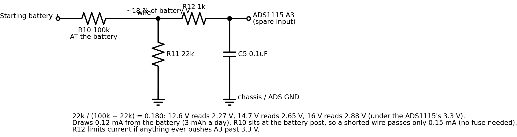
What it does. The ADS1115 can only read up to 3.3 V. The divider scales the battery to 18 %: 12.6 V reads 2.27 V, 14.7 V reads 2.65 V. This replaces the INA238 reading, which moves to the house bank in build C.
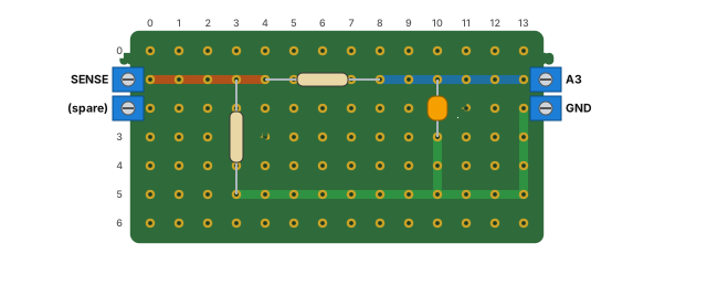
| Ref | Part | Holes |
|---|---|---|
| R11 | 22 kΩ (red-red-orange) | (3,1)–(3,5) |
| R12 | 1 kΩ | (4,1)–(8,1) |
| C5 | 0.1 µF | (10,1)–(10,3) |
| J5, J6 | 2-pin terminals | (0,1)–(0,2), (13,1)–(13,2) |
Back-side runs: (0,1)→(4,1) · (8,1)→(13,1) · (3,5)→(13,5)→(13,2); (10,3)→(10,5). J5's second pin isn't used.
- Test on the bench: put 12 V through R10 into J5 SENSE, with the 12 V negative on J6 GND. J6 A3 should read 12 × 0.18 ≈ 2.16 V.
- In the Jeep: J6 A3 to the ADS1115's A3, J6 GND to the ADS1115's GND. Then add the reading to the software and calibrate it once against a multimeter.
Board C: UPS feed (house bank to the X1209)
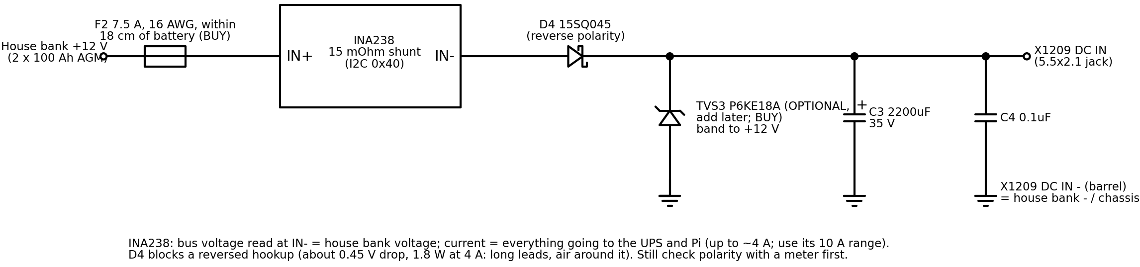
What it does. Powers the X1209 UPS from the AGM house bank all the time, so its cells stay full and the Pi can stay on while parked. The INA238 sits in this wire to read the bank's voltage and how much power the Pi uses. This is the only build carrying real current (up to 4 A), so it has two heavy rails and screw terminals, plus a fuse near the battery.
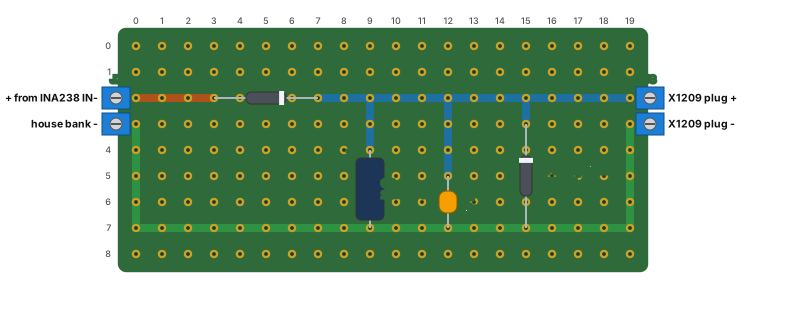
ELEGOO 3 × 7 cm board (only 20 × 9 holes used). Left = from the INA238 and house bank, right = to the X1209's DC plug.
| Ref | Part | Holes | Notes |
|---|---|---|---|
| D4 | 15SQ045 (the big axial diode) | (3,2)–(7,2) | Band at (7,2), toward the X1209. Its legs are thicker than the holes: open those two holes with a 1.3 mm (1/16") drill bit by hand. Keep the body off the board surface for air. |
| C3 | 2200 µF 35 V electrolytic | (9,4) +, (9,7) − | The stripe on the can is negative. Lay it on its side if it won't stand. |
| C4 | 0.1 µF ceramic | (12,5)–(12,7) | |
| TVS3 | P6KE18A (optional, buy later) | (15,3)–(15,7) | Band at (15,3), the + side. Leave the holes empty for now. |
| J7 | 2-pin terminal | (0,2) and (0,3) | + from the INA238 IN−, and house bank − |
| J8 | 2-pin terminal | (19,2) and (19,3) | To the X1209 plug lead: + and − |
| Back-side run | Holes (corners) | Heavy? |
|---|---|---|
| In + | (0,2)→(3,2) | Yes |
| +12 V out | (7,2)→(19,2); (9,2)→(9,4); (12,2)→(12,5); (15,2)→(15,3) | Yes: the row-2 run |
| Ground | (0,3)→(0,7)→(19,7)→(19,3) | Yes |
- Fuse first: the 7.5 A fuse holder goes within 18 cm (7 in) of the house bank + post. Leave the fuse out until the end.
- 16 AWG from the fuse to the INA238 IN+ terminal. From the INA238's IN−, an 18 AWG pigtail to J7 +. Run the house bank − to J7 − (the chassis works if the bank's − is grounded to it).
- Build Board C as drawn: D4 first (band toward the right), then C3 and C4, then the terminals, then the heavy back-side runs.
- From J8, an 18 AWG pair to the X1209's DC plug (5.5 × 2.1 mm): J8 + to the centre pin, J8 − to the sleeve. Check the polarity with the meter before plugging in.
- Before the fuse goes in: meter between J8 + and J8 − with no power should read open. Insert the fuse and J8 should read about +12 V (and under 14.8 V when the alternator charges the bank), not −12 V. Then plug it into the X1209.
- Set the INA238 to its ±10 A range in software. The ±2.75 A range would clip at 3-4 A.
Board D v2: amp remote turn-on (Pi GPIO 17)
Version 2, 14 Oct 2026. Replaces the first Board D (BC337 driver). Build it on a new board; don't modify the old one.
What it does. The Pi's amp controller (the jeep-startup service) drives GPIO 17, header pin 11: high turns the amps on, low turns them off. It switches on while music is playing, and turns off after 30 seconds of silence and when the Jeep is parked. This board puts +12 V on the amps' remote turn-on wire when the pin goes high, and 0 V when it is low or the Pi is off.
What changed from the first version
- Optocoupler drive. A PC817 (the same chip as Board A) replaces the BC337. The Pi side and the Jeep side share no wire on this board, so nothing on the 12 V side can reach GPIO 17.
- Bleeder on REMOTE. R4 (10 kΩ) holds REMOTE at 0.00 V when the board is off. The first version left REMOTE floating, so a meter could show stray voltages that meant nothing.
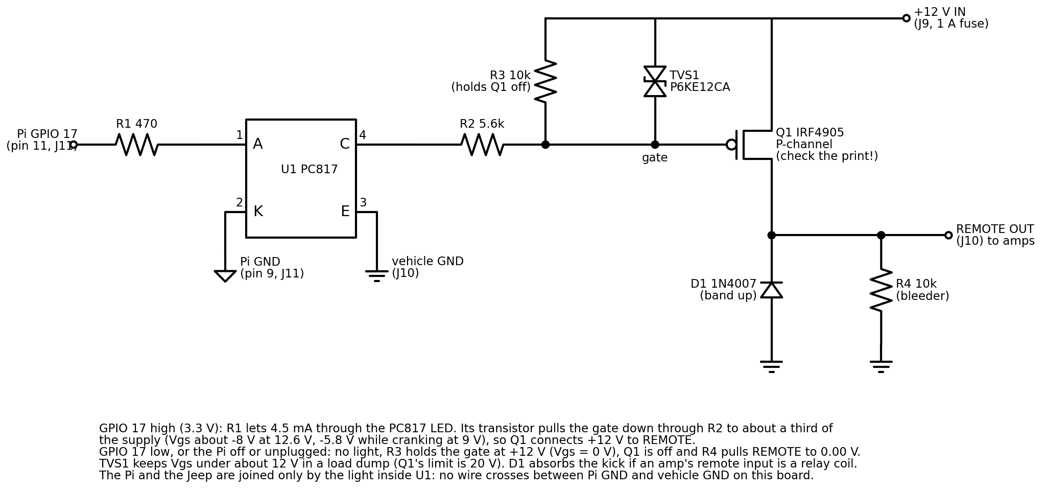
- Gate clamp. TVS1 keeps Q1's gate within about 12 V of its source, even in a 40 V load dump (Q1's limit is 20 V).
- Spaced layout. No two different connections sit in side-by-side holes, except the legs of one part.
board_layout.pynow checks this. The first layout had 13 such spots, two of them between the REMOTE wire and +12 V or the gate.
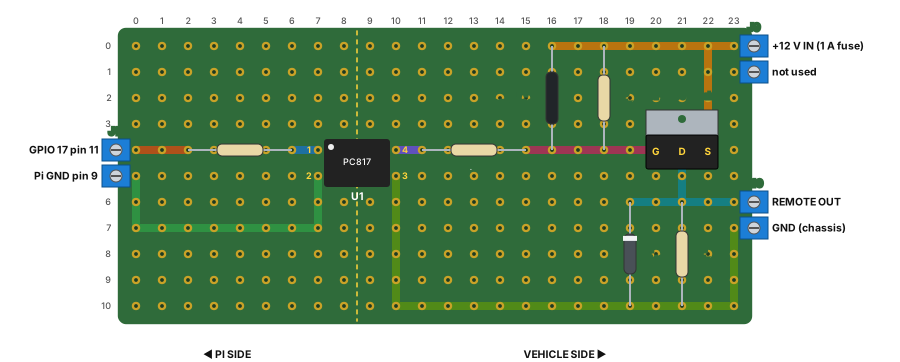
ELEGOO 5 × 7 cm board (24 × 18 holes; only the top 11 rows are used, so the rest can stay empty or be cut off). Left of the dashed line = Pi side, right = Jeep side.
- GPIO 17 high (3.3 V): R1 lets about 4.5 mA through the PC817's LED. Its transistor pulls Q1's gate down through R2 to about a third of the supply: 8 V below the source at 12.6 V, and still 5.8 V below while cranking at 9 V. Q1 connects +12 V to REMOTE.
- GPIO 17 low, Pi off or J11 unplugged: no light, so R3 holds the gate at +12 V. Q1 is off and R4 pulls REMOTE to 0.00 V.
- D1 catches the voltage kick if an amp's remote input is a relay coil.
Parts for Board D v2
| Ref | Part | Holes | Notes |
|---|---|---|---|
| U1 | PC817 | pin 1 at (7,4) | Dot top-left, the same way as on Board A. |
| R1 | 470 Ω (yellow-violet-brown) | (2,4)–(6,4) | LED current |
| R2 | 5.6 kΩ (green-blue-red) | (11,4)–(15,4) | Pulls the gate down when U1 is on |
| R3 | 10 kΩ (brown-black-orange) | (18,0)–(18,4) | Holds Q1 off |
| R4 | 10 kΩ (brown-black-orange) | (21,6)–(21,10) | Bleeder: REMOTE to ground |
| TVS1 | P6KE12CA | (16,0)–(16,4) | Either way round. It sits gate-to-source and sees at most about 9.4 V in normal use (at 14.7 V charging), under its 10.2 V standoff, so it doesn't conduct there. |
| Q1 | IRF4905 (P-channel MOSFET, TO-220) | G (20,4), D (21,4), S (22,4) | Metal tab toward the top edge, printed face toward the bottom edge. Read from the printed face with the legs down, they are G, D, S left to right. Leave about 3 mm of leg above the board. |
| D1 | 1N4007 | K (19,6), A (19,10) | Band at the top, (19,6). A 1N4001 also works, but the 1N4007 is rated 1000 V instead of 50 V. |
| J9 | 2-pin terminal | (23,0), (23,1) | +12 V in through a 1 A inline fuse. The second pin is not connected. |
| J10 | 2-pin terminal | (23,6), (23,7) | REMOTE out to the amps, and chassis ground. This is the board's only ground connection. |
| J11 | 2-pin terminal | (0,4), (0,5) | GPIO 17 (header pin 11) and Pi ground (header pin 9) |
| Back-side run | Holes (corners) |
|---|---|
| GPIO 17 | (0,4)→(2,4) |
| LED + | (6,4)→(7,4) |
| Pi GND | (0,5)→(0,7)→(7,7)→(7,5) |
| Collector | (10,4)→(11,4) |
| Gate | (15,4)→(20,4) |
| +12 V | (23,0)→(16,0); (22,4)→(22,0) |
| REMOTE | (21,4)→(21,6); (19,6)→(23,6) |
| Vehicle GND | (23,7)→(23,10)→(10,10)→(10,5) |
Build
- Read Q1's print: IRF4905. Set it aside from the IRLZ44Ns.
- Solder U1 first while the board is empty, dot top-left.
- Fit R1 to R4, then D1 (band at the top), then TVS1.
- Fit Q1 with the tab toward the top edge. Solder each leg separately, so no solder joins two legs.
- Fit the three terminals.
- Wire the back one run at a time, ticking each off against the list. Nothing here carries more than about half an amp, so clipped component legs are fine.
- Look at the back under a light, especially around Q1's three legs and the REMOTE run below them. No solder may join two different colours.
Meter checks before power
Board unpowered, nothing connected to any terminal.
| Check | Meter mode | Red lead | Black lead | Good reading | If not |
|---|---|---|---|---|---|
| 1. Isolation | Continuity | Each J11 pin | Each J9 and J10 pin | No beep | Solder or a wire crosses the dashed line |
| 2. Q1 is the right part | Diode | J10 REMOTE | J9 +12 V | 0.4–0.6 V | OL: Q1 is in backwards or a leg isn't soldered |
| 3. Q1 is the right part | Diode | J9 +12 V | J10 REMOTE | OL | 0.4–0.6 V: Q1 is an N-channel part (IRLZ44N). Swap in an IRF4905. |
| 4. Gate pull-up | Ohms | Q1 source leg | Q1 gate leg | 9.5–10.5 kΩ | Near 0: gate bridged to +12 V. Open: R3 not connected. |
| 5. Bleeder | Ohms | J10 REMOTE | J10 GND | 9.5–10.5 kΩ | Much lower: a bridge to ground. Open: R4 not connected. |
| 6. LED | Diode | J11 GPIO | J11 GND | about 1.0–1.8 V, OL reversed | OL both ways: U1 turned round, or R1 open |
Bench test with power
12 V through the 1 A fuse to J9 +12 V, its negative to J10 GND. Nothing on REMOTE except the meter.
- Off. J10 REMOTE to J10 GND: 0.00 V (under 0.05 V). Red on Q1's source leg, black on its gate leg: 0.0 V.
- On. Put 3 to 3.3 V on J11: the Pi's pin 1 to J11 GPIO and pin 9 to J11 GND, or two AA cells, + to GPIO. REMOTE should read within 0.1 V of the supply (12.5 V or more at 12.6 V). Source to gate should read about 8 V.
- Under load. Add a 1 kΩ resistor or a small 12 V bulb from REMOTE to J10 GND. With 3.3 V on J11, REMOTE stays within 0.1 V of the supply. With it removed, REMOTE falls to 0.00 V within a second.
In the Jeep
- Shut the Pi down. J11 to header pin 11 (GPIO 17) and pin 9 (GND).
- J9 +12 V through the 1 A inline fuse. J10 GND to chassis. J10 REMOTE to the amps' remote wire, after taking that wire off whatever fed it before.
- Boot the Pi: the amps stay off. Play music: they turn on. Stop: they turn off about 30 seconds later.
If it misbehaves
| Symptom | Measure | Cause |
|---|---|---|
| REMOTE has 12 V with GPIO 17 low or J11 unplugged | Source to gate about 0 V | Q1 is the wrong part (meter check 3), or solder joins +12 V to the REMOTE run near Q1's legs |
| Source to gate about 8 V | U1 is switched on: U1 turned round, or the collector run (10,4)–(11,4) touches ground | |
| REMOTE stays at 0 V with 3.3 V on J11 | U1 pin 4 to J10 GND stays near +12 V | The LED isn't lit: check R1 and U1's orientation (meter check 6) |
| U1 pin 4 near 0 V, but source to gate under 2 V | R2 open, or the gate run doesn't reach Q1 | |
| Source to gate about 8 V | Q1 in backwards, or its drain leg isn't soldered | |
| REMOTE drops below 11 V once the amps are connected | J9 +12 V to J10 GND under load | A weak +12 V feed (fuse holder or wire), not the board |
ltspice\boardD_v2.cir, boardD_v2_surge.cir, r2_compare.cir and swap_check.cir.Board E: battery isolator solenoid driver
What it does. The isolator solenoid joins the starting battery to the house bank while the Jeep is running, and splits them when it isn't. This small board closes that switch whenever the accessory wire is live: ACC on lights a MOSFET (a transistor used as a switch) that connects the solenoid coil's negative side to ground. The coil's positive side goes straight to a fused +12 V, not through the board.
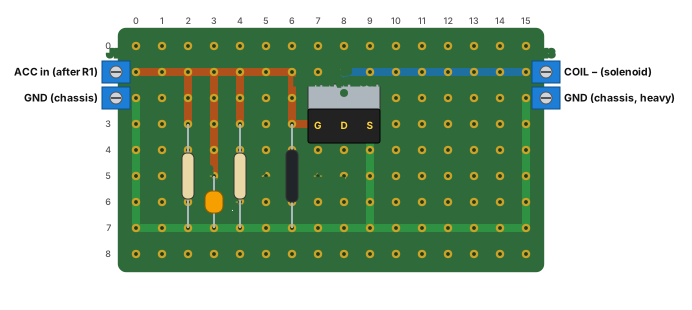
ELEGOO 3 × 7 cm board (16 × 9 holes used). Left = ACC in, right = the solenoid's coil −.
- How it works: ACC (9 to 14.7 V) reaches the gate through R1 5.6 kΩ, which sits at the ACC tap end of the wire (it limits current if the wire ever shorts), then R2 10 kΩ. R1 and R2 divide the voltage to about 64 % of ACC, so the gate sees about 9.4 V at 14.7 V and 5.8 V at 9 V while cranking. The IRLZ44N is fully on from about 5 V. ACC off or the wire disconnected: R2 holds the gate at 0 V and the MOSFET is off.
- TVS (P6KE12CA, gate to ground) stays off in normal use (the gate never exceeds about 9.5 V, under its 10.2 V standoff) and clamps spikes so the MOSFET gate (limit ±20 V) is safe. C1 smooths noise.
- Current: the coil current passes through Q3, the ground rail and the J13/J12 ground terminals. Measure the isolator's coil resistance before trusting any figure: the plain (non-smart) Recoil may draw 3 to 6 A, and the MOSFET then dissipates 0.2 to 0.8 W. Bolt a small TO-220 heatsink to Q3 (or add a second IRLZ44N in parallel) if it gets too hot to touch. Over 10 A, switch to a relay or a bigger MOSFET. The big 500 A current flows between the battery posts, never through this board.
| Ref | Part | Holes | Notes |
|---|---|---|---|
| Q3 | IRLZ44N (N-MOSFET, TO-220) | G (7,3), D (8,3), S (9,3) | Metal tab toward the top edge, printed face toward you. G, D, S read left to right. |
| R2 | 10 kΩ (brown-black-orange) | (2,3)–(2,7) | |
| C1 | 0.1 µF ceramic | (3,5)–(3,7) | |
| R3 | 100 kΩ (brown-black-yellow) | (4,3)–(4,7) | A backup pull-down: if R2 ever opens, this still holds the gate off. |
| TVS | P6KE12CA | (6,3)–(6,7) | Either way round (bidirectional). |
| R1 | 5.6 kΩ (green-blue-red) | off the board | Solder it in the ACC wire right at the tap, with heatshrink, like the other far-end resistors. |
| J12 | 2-pin terminal | (0,1), (0,2) | ACC in (after R1) and chassis ground |
| J13 | 2-pin terminal | (15,1), (15,2) | COIL − from the solenoid, and a second chassis ground (the heavy one) |
| Back-side run | Holes (corners) | Heavy? |
|---|---|---|
| Gate (ACC) | (0,1)→(6,1)→(6,3)→(7,3); (2,1)→(2,3); (3,1)→(3,5); (4,1)→(4,3) | No |
| Coil − | (15,1)→(8,1)→(8,3) | Yes |
| Ground | (0,2)→(0,7)→(15,7)→(15,2); (9,3)→(9,7) | Yes: the part from (9,7) to (15,7) and up to J13 |
- Fit R2, C1, the TVS, then Q3 (tab to the top edge), then the two terminals. Wire the back as listed. Lay a bare 18 AWG wire along the heavy runs and solder it at every hole, the same as Board C.
- Solenoid wiring: coil + stays wired to the battery as it is now. A 3 A inline fuse within 18 cm of the battery post is worth adding if it has none, sized for the coil current you measure (3 A is only enough if it is under 2 A; use 7.5 A for a 5 A coil). Coil − goes to J13 pin 1. Use 18 AWG for the coil wires (the terminals take 18 AWG at most and are rated 6 A).
- ACC wire: tap an accessory circuit that is already fused. Solder R1 (5.6 kΩ) into the tap end of the wire, cover it with two layers of heatshrink, and run the wire to J12 pin 1. J12 pin 2 goes to chassis ground.
- Bench test with the solenoid unplugged: put a 12 V source on ACC through R1 and measure the gate at (7,3) with a meter to ground: about 7.7 V from 12 V, and 0 V with ACC off. Then connect a small 12 V lamp or relay coil between +12 V and J13 pin 1: it should light when ACC is on and go dark when ACC is off.
- Connect the solenoid, then turn the key to ACC: you should hear it click closed. Key off: it opens.
Cranking: many vehicles drop the ACC wire while the starter turns, so the isolator opens for a second or two and closes again when the key returns to RUN. That is one open and one close per start, not chatter.
Reverse polarity: the solenoid's built-in diode would short a reversed battery connection, so keep a small fuse (3 A) in the coil's positive wire, near the battery. If it isn't fused today, add one.
Pi wiring
Use female jumper (Dupont) leads from the screw terminals to the Pi's 40-pin header. Each half of Board A has its own 3.3 V and GND pin, so no wires need to be shared.
| Terminal | Pi header pin | Signal |
|---|---|---|
| J2 3.3V | pin 1 | 3.3 V |
| J2 GPIO12 | pin 32 | GPIO 12 (tach) |
| J2 GND | pin 34 | Ground |
| J4 3.3V | pin 17 | 3.3 V |
| J4 GPIO10 | pin 19 | GPIO 10 (ACC) |
| J4 GND | pin 20 | Ground |
| J6 A3 / GND | ADS1115 A3 / GND | Starting battery |
| J11 GPIO17 | pin 11 | Amp remote (already used by the amp controller) |
| J11 GND | pin 9 | Ground |
Gemini check
Gemini 3.1 Pro reviewed all four circuits on its own, without seeing the designer's answers, and looked up the X1209's specs online.
| Circuit | Gemini | What it confirmed or changed |
|---|---|---|
| Tach | OK | Same LED currents, and the filter is fast enough at 6000 rpm. Count the falling edge of GPIO 12 (the spark moment). The PC817 switches in about 20 µs against a 2500 µs period at top RPM. |
| ACC | OK | A resistor at the tap instead of a fuse is standard practice for sense wires. In an extreme 100 V surge R5 could burn open, which is a safe way to fail. |
| UPS feed | Changed | Don't use two P6KE12CA in series; leave the TVS out until a P6KE18A is bought. Show the negative return wire (added). The 15SQ045 is fine at 1.8 W in free air. |
| Start battery | OK | About 0.1-0.3 % reading error from the ADS1115's input, which calibration removes. A 40 V surge pushes only 0.19 mA into the ADS1115 (its limit is 10 mA), and it's harmless with the Pi off. |
Gemini's X1209 facts were checked against Geekworm's own listing (6-18 V on a 5.5 × 2.1 mm jack, 12 V 3 A recommended). Its one claim that couldn't be confirmed, about what the Geekworm wiki says on input protection, was left out.